
NVIDIA Ampere announcement
From general purpose GPUs to AI supercomputers
NVIDIA has always been synonymous with high-performance graphics cards (GPU). In 2007, they introduced the CUDA programming environment for general purpose graphic cards (GP GPU), making it a major player in accelerated computing for HPC (High Performance Computing) applications, data analysis, and more recently algorithms for artificial intelligence (AI). Since that NVIDIA has introduced a range of hardware and software technologies to further accelerate computing, and its accelerators have become the main computing power of the world’s most powerful supercomputers – IBM’s #1 Summit and #2 Sierra are built on NVIDIA Tesla V100 chips.
GTC 2020
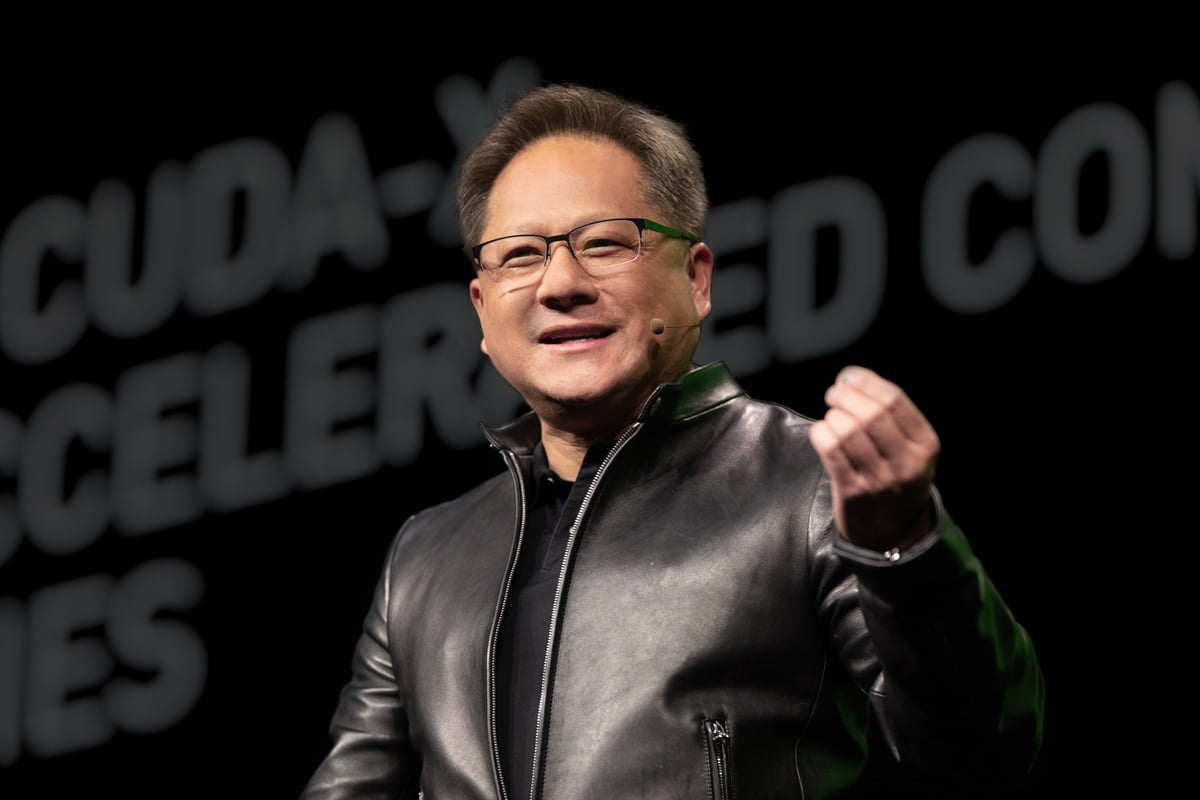
The GPU Technology Conference (GTC) is the world’s largest conference on graphics cards, accelerated computing and, in recent years, artificial intelligence. Regularly, the greatest interest is in the Jensen Huang’s keynote, who in his typical black leather jacket presents news and trends in the areas in which NVIDIA offers its products. It has been three years since the announcement of the breakthrough accelerator NVIDIA Tesla V100, so this year we were eagerly awaited what they had baked in NVIDIA. Jensen’s presentation begins traditionally … I AM AI.
NVIDIA Ampere
After watching the video from Jensen’s kitchen, it is clear that the biggest news of this year’s presentation will be the GPU architecture of NVIDIA Ampere, the NVIDIA A100 accelerator, which is built on this architecture, and the DGX A100 system. DGX A100 is a reference architecture of a tuned system for AI and HPC calculations, equipped with eight NVIDIA A100 accelerators. In his video, Jensen takes the system board with these eight GPU accelerators out of the oven and introduces it as the most powerful accelerator in the world.
NVIDIA A100
The NVIDIA A100 accelerator is manufactured using 7 nm technology in the TSMC factory. It contains over 54 billion transistors on an area of 826 mm2. The main technological innovations of the new chip include:
- Tensor cores (3rd generation) optimized for HPC calculations and AI
- 40 GB fast HBM2 with 1.6 TB/s throughput, 40 MB L2 cache
- Multi-Instance GPU (MIG) for multi-user work with a single card
- faster NVLINK for interconnection of multiple cards (600 GB/s per card)
- PCIe gen4 bus for connection to CPU and network cards (31.5 GB/s)
Improvements of Tensor cores in FP64 (double precission) computations greatly helps computational performance in traditional HPC computations and simulations, while support for TF32 and BF16 accelerates training and subsequent application (inference) of neural networks. The maximum theoretical performance for the individual accuracies of the calculation is showed in the table on the right. The stated values take into account the Boost frequency of the computational cores. NVIDIA also introduced Fine grained structured sparsity for working with deep neural networks. Thanks to it, it is possible to double the stated performance values!
Comparison of NVIDIA A100 with existing accelerators
In general, the NVIDIA A100 accelerator is the most powerful hardware on which demanding computing tasks can be processed.
| ParametEr | Tesla T4 | Tesla V100 SXM2 | A100 SXM4 | DGX-1 | DGX-2 | DGX A100 |
|---|---|---|---|---|---|---|
| Architecture | Turing | Volta | Ampere | Volta | Volta | Ampere |
| Nr. of CUDA Cores | 2 560 | 5 120 | 6 912 | 40 960 | 81 920 | 55 296 |
| Nr. of Tensor Cores | 320 | 640 | 432 | 5 120 | 10 240 | 3 456 |
| FP64 Performance | 0,25 TFLOPS | 7,8 TFLOPS | 9,7 TFLOPS | 62 TFLOPS | 125 TFLOPS | 77,6 TFLOPS |
| Tensor (FP64) Performance | — | — | 19,5 TFLOPS | — | — | 156 TFLOPS |
| FP32 Performance | 8,1 TFLOPS | 15,7 TFLOPS | 19,5 TFLOPS | 125 TFLOPS | 250 TFLOPS | 156 TFLOPS |
| Tensor (TF32) Performance | — | — | 156 TFLOPS | — | — | 1,2 PFLOPS |
| Tensor (FP16) Performance | 65 TFLOPS | 125 TFLOPS | 312 TFLOPS | 1 PFLOPS | 2 PFLOPS | 2,5 PFLOPS |
| GPU Memory | 16 GB | 32 GB | 40 GB | 256 GB | 512 GB | 320 GB |
| Memory Technology | GDDR6 | HMB2 | HMB2 | HMB2 | HMB2 | HBM2 |
| Memory Throughput | 300 GB/s | 900 GB/s | 1 ,5 TB/s | 900 GB/s | 900 GB/s | 1,5 TB/s |
| GPU card interconnection | none | NVLink | NVLink3 | NVLink, hypercube topologie | NVSwitch, non-blocking | NVSwitch3, non-blocking |
| Maximum power consumption | 70 W | 300 W | 400 W | 3 500 W | 10 kW | 6,6 kW |
| Form Factor | PCIe card | SXM2 card | SXM4 card | rack, 3U | rack, 10U | rack |
| On the Market since | 2018 | 2017 | 2020 | 2017 | 2018 | 2020 |
We reviewed the current CPU platforms (Intel, AMD, POWER and ARM) in the March Comparsion of Server Processors. We are also preparing a comparison of accelerators for HPC and AI.


NVIDIA DGX A100
When announcing the previous generation of Tesla accelerators, NVIDIA also introduced reference systems optimized for HPC and AI calculations – NVIDIA DGX. With the introduction of the NVIDIA A100 accelerator, a new DGX system – the NVIDIA DGX A100 – was also introduced.

Along with the DGX A100 system, NVIDIA also introduced the HGX A100 system, a system board equipped with four or eight NVIDIA A100 accelerators that OEM and ODM server manufacturers integrate into their systems. HPE, Gigabyte and Supermicro should be among the first manufacturers of these systems.


